


A page from the "Causes of Color" exhibit...
Why are cinnabar, vermilion and cadmium colored? (pure semiconductors)

|
|||||||||||||||||||||||||||||||||||||||||||||||
Above table shows the relationship between the size of the band gap in a semiconductor and its color.

These silicon wafers, which will be cut up and used in electronic devices, illustrate the metallic appearance of typical semiconductor materials. The surface is overlaid with laboratory-grown microelectronic circuitry.
A painter’s palette is rich with colors, some of which arise from the band gaps in natural semiconductors.
The mechanism behind the color we perceive in semiconductors can be explained by the band theory that governs color in many metals. Like metals, semiconductors have a reflective surface when polished, but they do not conduct electricity as effectively. In fact, semiconductors frequently act as insulators, and require particular conditions in order to become conductors. While metals become more resistant to the flow of charge with increasing temperature, semiconductors become conductors only with sufficient thermal energy, performing better as temperature increases.
According to band theory, the electrons in some solids behave differently than those in individual atoms. In a single atom, an electron can occupy one of several distinct energy levels. When light strikes the surface, electrons in a lower energy level can be excited to a higher energy level. The distance between the levels represents the relative energy required to excite an electron. As atoms are brought closer together, these distinct energy levels interact. The low energy levels overlap and the high energy levels overlap. As the number of neighboring atoms increases, more overlap occurs and bands of low and high energy replace the distinct energy levels.
The portion of the band below the level of the gap, called the valence band, contains a full complement of electrons in the absence of thermal energy. The portion of the band above the gap is known as the conduction band, because electrons excited to this level are available to conduct electricity. This leaves a positively charged "hole" in the valence band into which an electron can move, so that the valence band can also contribute to the flow of charge. However, unlike electrons in metals, electrons in semiconductors may not be re-emitted readily or immediately, so that absorption is always dominant over re-emission.
|
Comparing the energy band gap for insulators, semiconductors, and metals. Insulators have a band gap so large that electrons cannot cross it, while in metals there is effectively no gap. Semiconductors lie between these extremes. |
The absorption of light in a material with a band gap separating the valence electron energy level from the conduction band energy level (left), and the variation of color with the size of the band gap (right) |

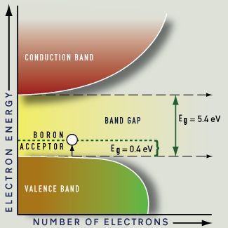
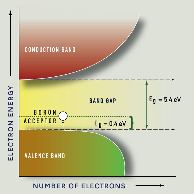
The portion of the band above the gap is known as the conduction band, because electrons excited to this level are available to conduct electricity. This leaves a positively charged "hole" in the valence band into which an electron can move, so that the valence band can also contribute to the flow of charge. A specific minimum energy is required to excite electrons across the energy gap from the valence band to the conduction band. This has important consequences for color. The magnitude of the energy spacing between the two bands is the "band gap" or "energy gap," usually designated Eg.
In this diagram, the vertical arrows A, B, and C represent the absorption of light. Since there are no electron energy levels in the band gap between the valence and conduction bands, the lowest-energy light that can be absorbed corresponds to arrow A. This is the energy required to excite an electron from the top of the valence band up to a level at the bottom of the conduction band. The energy required corresponds to the band-gap energy Eg. Light of higher energy can also be absorbed, as shown by arrows B and C.
If the substance has a large band gap, such as the 5.4 eV of diamond or the similar value of corundum, then no light in the visible spectrum can be absorbed. These substances transmit all incident light, and are colorless in their pure forms. In their powdered forms, or when their structure prevents light being transmitted, all light is reflected back to the observer and we see them as white. Such "large band gap semiconductors" are excellent insulators and behave like covalently bonded materials.
If a pigment is able to absorb all wavelengths, we see it as black, just as we see most metals as black in their powdered form. A white pigment absorbs no visible light. As in subtractive color mixing, when a specific wavelength is absorbed from incident white light, we see its complementary color.
A "medium band gap semiconductor" is a material with a somewhat smaller band gap, such as the compound cadmium sulfide (CdS). This is the pigment cadmium yellow, known as the mineral greenockite (more examples in table).
In cadmium yellow, the 2.6 eV band gap energy permits absorption of violet and some blue, but none of the other colors. Only light above 2.6 eV is absorbed. We see it as a yellow color, as shown by the color scale at the right of the diagram. A smaller band gap that permits absorption of violet, blue, and green produces an orange color. An even smaller band gap, as in the pigment vermillion (the mineral cinnabar, HgS) with a band gap of 2.0 eV, results in all energies but the red being absorbed, leading to a red color.
All light is absorbed when the band gap energy is less than the 1.77 eV (700 nm) limit of the visible spectrum. These "narrow band gap semiconductors" are black, as in the last three materials of the table.

Mixed crystals of yellow cadmium sulfide CdS and black cadmium selenide CdSe, showing the variation of colors as the band gap decreases
An illustration of this change in the band gap size is shown using mixed crystals of yellow cadmium sulfide (CdS, Eg = 2.6 eV), and black cadmium selenide (CdSe, Eg = 1 .6 eV), which have the same structure and form a solid-solution series. The photograph above illustrates the yellow-orange-red-black sequence of these mixed crystals as the band-gap energy decreases.
Mixed crystals such as cadmium sulfoselenide (Cd4SSe3) form the painter’s pigment cadmium orange, and are also used to color glass and plastic. Mercuric sulfide (HgS) exists in two different crystalline forms. Cinnabar (the pigment vermillion) with Eg = 2.0 eV is a deep red, but can transform upon exposure to light in an improperly formulated paint to the black metacinnabar with Eg = 1.6 eV in as little as five years; this has happened in a number of old paintings.
Another method of manipulating the color of semiconductor materials is by adding impurities. These doped semiconductors have energy levels within the band gap, and allow us to tailor the wavelength of emitted light. Some semiconductors contain impurities in their natural state, providing useful insights into these behaviors.